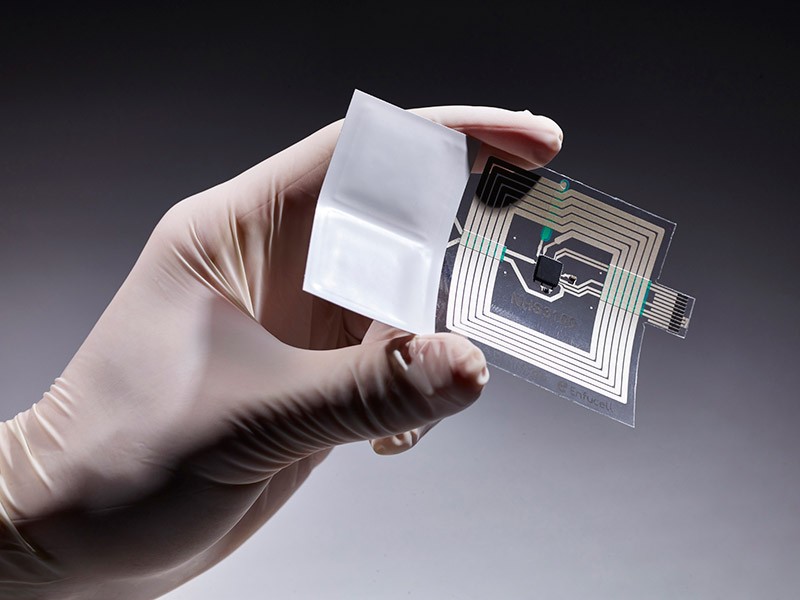
In Mold Electronics (IME) is making a commercial comeback. The behind-the-scenes interest in IME remains robust. The first wave of products are close to market launch, the value networks are being enhanced, volume manufacturers are more engaged than ever, and the material set is transitioning beyond conductive inks to include transparent conductive films, sensors, actuators, and so on. Overall, we expect 2017/18 to the years when IME applications finally grow after years of on and off starts.
Transition beyond components-in-a-box
IME enables the manufacture of structural electronics where the electronics are part of the structure itself. It leads to more elegant space-saving designs where discreet components such as PCBs become redundant, and helps the industry transition beyond the current old-electronics-in-a-new-box approach. This technology is currently best suited to high-volume and low-complexity applications particularly in sectors such as whitegoods and automotive. Note that IME is distinct from MID (Molded Interconnect Devices). In the former, the graphical and functional layers are first deposited (e.g. printed) on a flat 2D surface and then formed into a 3D object; whereas in the latter the 3D object is first formed and then metallized using processes such as LDS (laser direct structuring). The IME process is still relatively immature. The industry had largely been pushed along by material suppliers in search of new market outlets, particularly conductive paste makers. The manufacturing step of the value chain had remained weak and most progress, until recently, had been made at piloting facilities by small- to medium-sized firms.
This is changing now as we witness strong engagement from large contract manufacturers. The processing know-how is also accumulating and the industry is learning how to optimize the many trade-offs involved in going from a pilot design to one streamlined for mass manufacture. The cost of production is still higher than the incumbent solution therefore IME products must create additional value such as better aesthetics or thinner designs. This state, however, is likely to be temporary and we anticipate that IME will, in the long run, become cost competitive with incumbent solutions: little intrinsic technological barrier exists to prevent this. The reliability also remains unproven, particularly compared to tried and tested PCB-based solutions. This creates an additional risk for end users particularly for high-volume and long-life products. This, too, is expected to change over the coming years as this emerging value chain accumulates more experience.
Novel material challenges
The IME is a new process for functional materials beyond graphical inks that establishes a new set of performance requirements for IME-compatible materials. These new or modified materials, for example, need to withstand a large non-recurring elongation event during the forming process. These materials will also almost always exist within a stack of materials, all of which need to be optimized for IME compatibility. Conductive pastes and adhesives were the first functional material to be developed specifically for IME compatibility. The early works were demonstrated more than five years ago. The industry has refined the formulations based on market and technical feedback, whilst the supplier base has rapidly increased. Indeed, in the early days, the ability to work with customers to customize inks would win contracts, but in the medium term this product too will become largely commonplace and gradually lose its price premium compared to better established and more mature conductive paste products.
Expanding toolkit of materials
The functional material’s menu is now fast expanding, transitioning beyond conductive pastes to include transparent conductive films, sensors, and actuators and so on. The images below, taken at various conferences by my colleagues and I, demonstrates this trend. This inevitably opens up more applications options beyond structurally-integrated interconnects that seek to replace discreet PCBs. Take transparent conductive films as an example. Here, various technology options such as carbon nanotubes (CNTs), PEDT and even metal mesh have been shown to be thermoformable. These technologies are opening up new applications such as 3D touch surfaces for whitegoods and automotive infotainment systems. Here too material suppliers are pushing to establish the entire value chain and to prove the reliability of their application ideas. The material kit will soon transition even beyond TCFs to include, for example, haptics/sensors. We have already witnessed prototype-level work on over-moulding polymeric haptics/sensors. We expect this development to help transition this material class, and similar ones, into ones that can be directly moulded into 3D shapes.


